

Announcements MORE
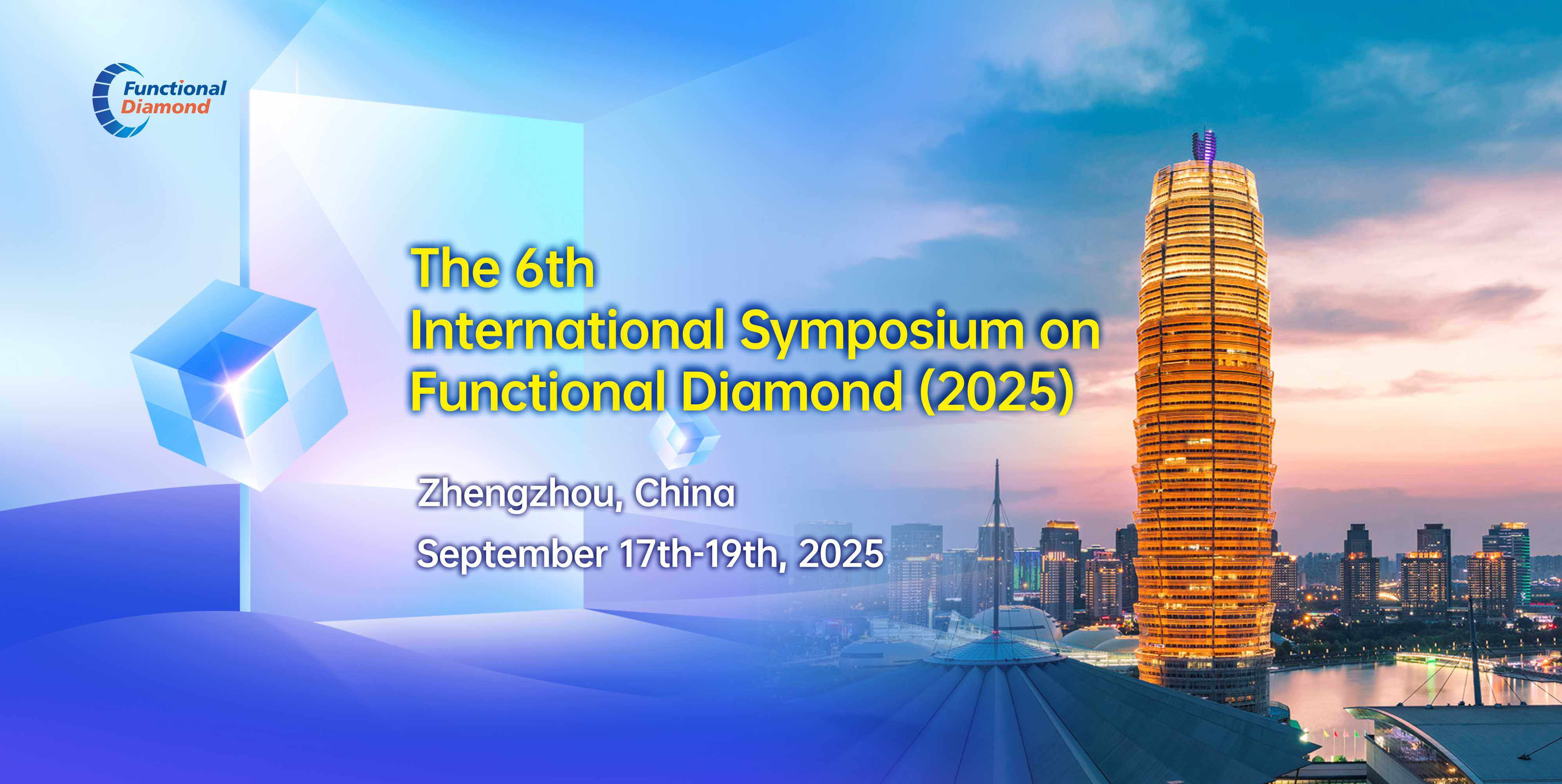
- The 6th International Symposium on Functional Diamond (2025) 2025-02-27
- The 5th International Symposium on Functional Diamond (2024) 2024-09-30
- Functional Diamond Accepted into ESCI in Web of Science 2024-06-12
- Call for paper | Special Issue on Advances in Diamond Photonics 2024-05-08
- 2023 Conference on Diamond Industry 2023-07-24
Entrance
Journal Published by Taylor & Francis Group Submit Review
Editor's choice articles
MOREHigh-power dual-wavelength intracavity diamond Raman laser
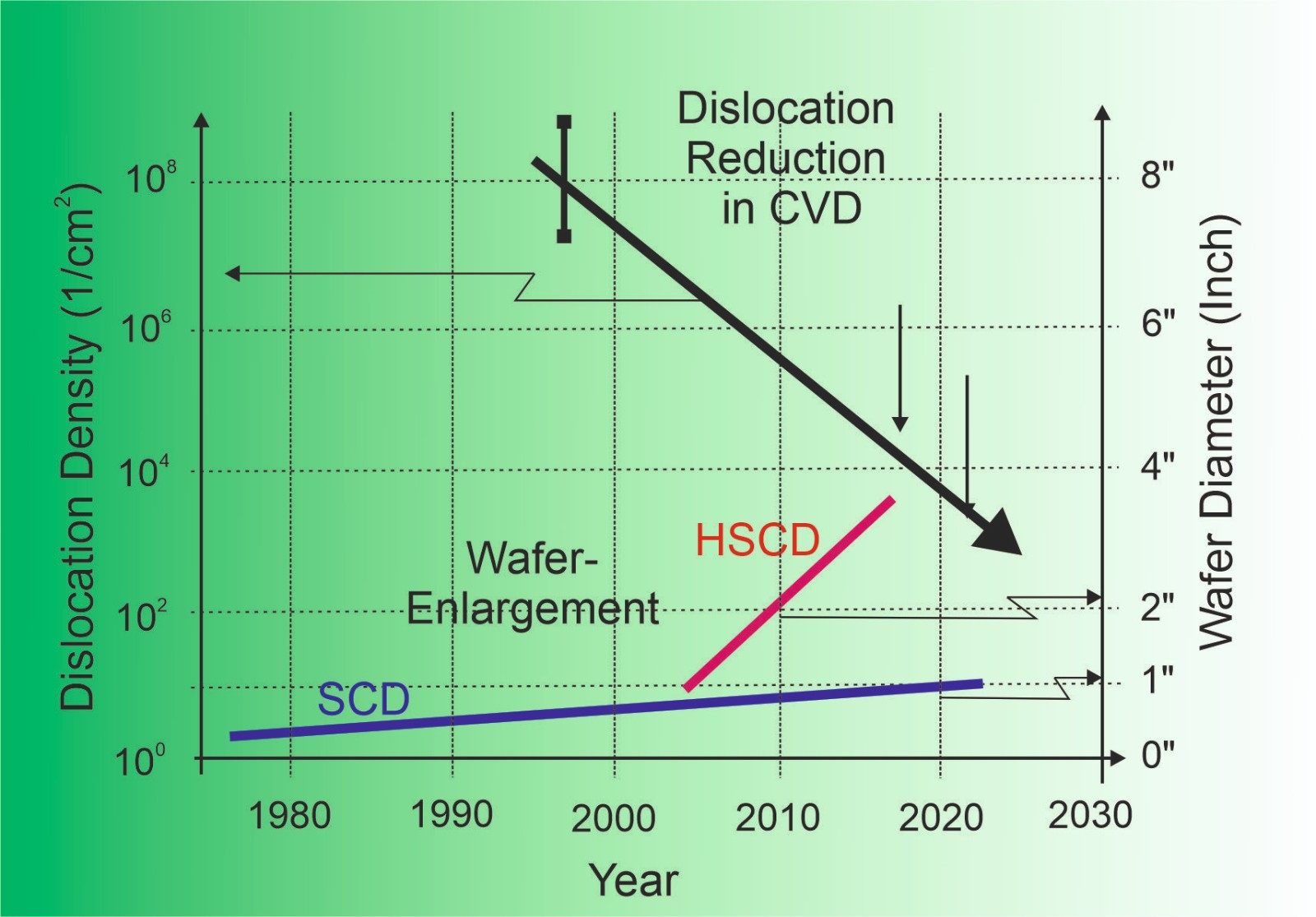
Effect of step-flow modulation on the large-size single crystal diamond through mosaic growth
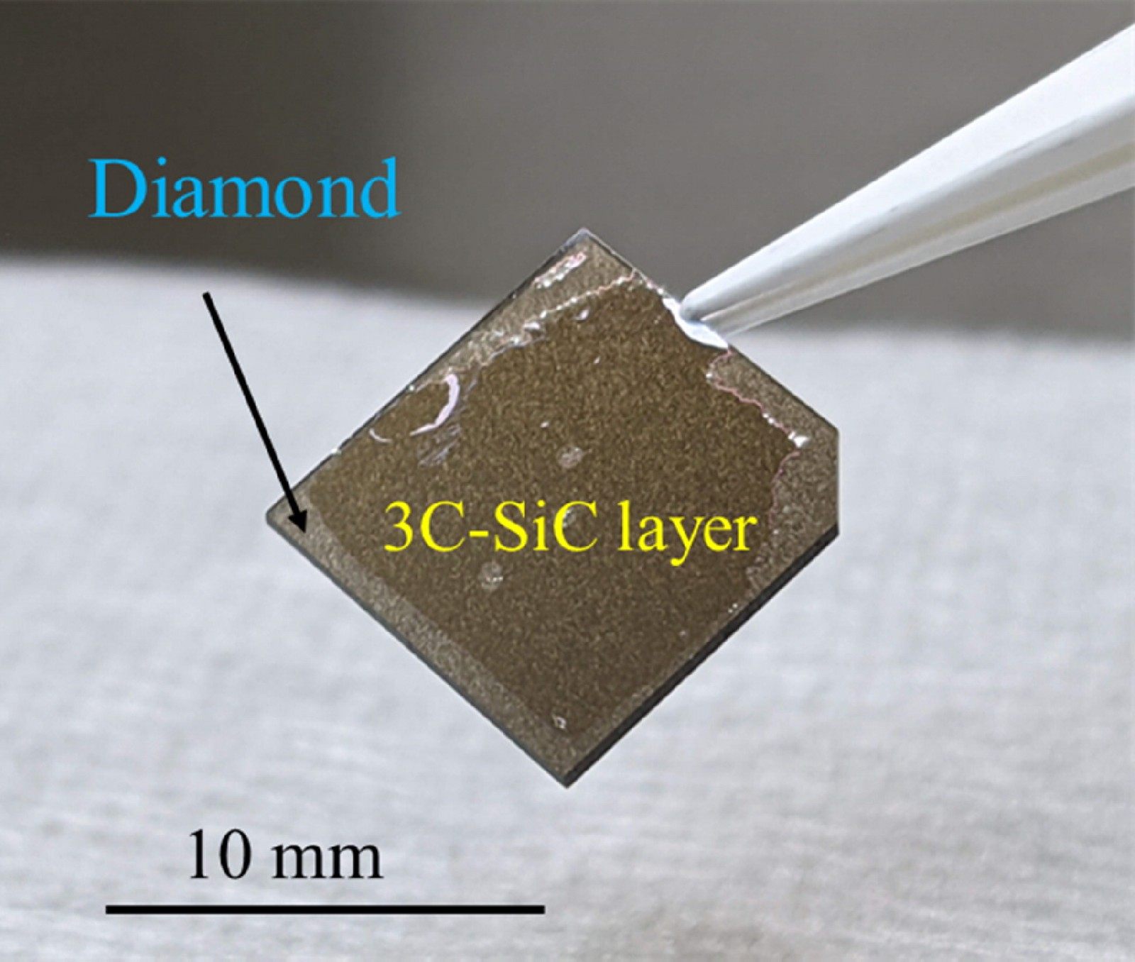
Single-crystal diamond growth by hot-filament CVD: a recent advances for doping, growth rate and defect controls
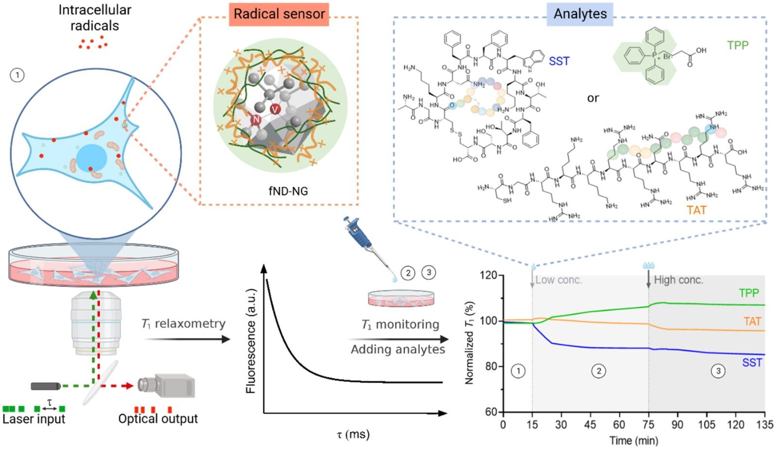
Tailoring optical emission of silicon-vacancy centers in two-dimensional diamond nanosheets via a two-step oxidation approach
Latest articles
- Abstract:This paper proposes a hydrogen-terminated diamond MOSFET structure with a buried N-layer and systematically studies its static and breakdown characteristics using Sentaurus TCAD. By introducing an N-type buried layer below the gate-drain channel, the internal electric field distribution of the device is effectively modulated, while new electric field peaks are formed within the drift region, achieving uniform distribution of the electric field between gates and drains. Simulation results show that the proposed structure can significantly increase the device breakdown voltage while having less impact on on-resistance, thereby achieving a higher Baliga’s figure of merit (BFOM).
- Abstract:Porous self-supported boron-doped polycrystalline diamond (P-BDD) bulk electrodes were directly fabricated from graphite and aluminum diboride (AlB2) through a one-step high-pressure high-temperature (HPHT) process, without prior synthesis of BDD particles or subsequent consolidation. The resulting P-BDD exhibited a diamond-dominant crystalline structure, porous morphology, and a room-temperature electrical resistivity of 1.66 × 10⁻³ Ω·m. Raman spectroscopy showed features consistent with boron incorporation, while Hall measurements confirmed p-type conduction with a hole-carrier concentration of 3.18 × 10²³ m−3. The electrode exhibited an electrochemical potential window of approximately 2.13 V in 0.5 M H2SO4 and maintained stable electrochemical performance during repeated cycling. In addition, the P-BDD electrode demonstrated improved thermal oxidation resistance, with an oxidation onset temperature of approximately 969°C. The electrochemical oxidation capability was evaluated using 60 mL of methylene blue solution (30 mg·L−1), achieving approximately 98% MB decolorization within 30 min under galvanostatic conditions. This work provides a direct one-step HPHT strategy for preparing porous BDD bulk electrodes with combined electrical conductivity, thermal stability, and electrochemical oxidation capability.
- Abstract:In this study, a single-crystal diamond (SCD) MEMS cantilever was fabricated using a buried graphite sacrificial-layer process. A region containing nitrogen-vacancy (NV) centers formed near the ion-implantation-induced defective layer was directly utilized as the stress-sensing region of the released cantilever, enabling dynamic stress sensing without the use of externally attached nanodiamonds. We investigated the relationship between the stress induced by the cantilever vibration and the peak shift of the fluorescence intensity of the optically detected magnetic resonance (ODMR) spectrum. By approximately aligning the static magnetic field with one of the four NV-center crystallographic axes, we were able to evaluate the dependence of the peak shift on stress. Our findings revealed that the peak shift can effectively detect uniaxial stress due to normal vibration. In addition, as the vibration amplitude increased, the magnitude of the ODMR peak shift also increased, showing a trend consistent with previously reported NV-center stress responses. Furthermore, the ODMR shift exhibited periodic modulation corresponding to the cantilever’s vibration phase. These results indicate that NV centers in micromachined SCD cantilevers can be used to detect vibration-induced dynamic bending stress.
- Abstract:Diamond surfaces terminated with a silicon layer (C–Si) can induce a two-dimensional hole gas (2DHG) layer at the insulator/diamond interface, enabling the realization of p-channel metal–oxide-semiconductor field-effect transistors (MOSFETs). Through two primary fabrication routes—namely, SiO2 annealing in a reducing atmosphere and silicon molecular beam deposition (MBD) at high temperatures—stable oxidized silicon-terminated (C–Si–O) and C–Si diamond channels have been realized. These channels facilitate normally-off p-channel FETs with threshold voltages (VTH) ranging from −3 to −16 V and hole mobilities between 100 and 200 cm2/V·s. For instance, a (111)-oriented C–Si–O MOSFET with a VTH of −5.6 V delivers an output current density of −311 mA/mm, whereas another MBD C–Si–O MOSFET with a varying source-to-drain distance (LSD) shows a ΔVTH shift whose magnitude is less than 0.2 V. This review provides a critical overview of the chemical structures, the formation methods, and operational mechanisms of C–Si–O diamond surfaces. It also summarizes recent progress in C–Si–O diamond electronic devices, with emphasis on device architectures, fabrication techniques, and electrical characteristics. Finally, key challenges and potential pathways toward the industrial adoption of this emerging technology are discussed.
- Abstract:Diamond possesses excellent physical and electronic properties, and demonstrates great application potential in the next-generation high-power and high-frequency power electronic devices. In recent years, significant progress has been made in the research on diamond diodes and field-effect transistors (FETs). This paper summarizes the effects of channel types, gate dielectrics, substrate types and device structures on the performance of diamond FETs and diodes. The hydrogen-terminated surface provides a high-performance channel for FETs through the formation of a two-dimensional hole gas, while Al2O3 and h-BN and other gate dielectric materials play a key role in reducing interface state density and improving the high-temperature stability of the devices. The development of high-quality 2-inch sapphire heteroepitaxial diamond substrates effectively alleviated the problem of size limitations of diamond substrates, providing a feasible solution for the fabrication of large-area and low-cost diamond devices. The article analyzes the factors that affect the core performance of diamond devices, including breakdown voltage, on-resistance, current density and threshold voltage. The field plate structure can alleviate the edge electric field concentration effect of the Schottky metal, effectively increase the breakdown voltage of the diamond Schottky diode, and does not sacrifice its forward characteristics. We discuss the main bottlenecks and challenges that currently restrict the development of diamond devices. We propose effective strategies to enhance the overall performance of diamond electronic devices from perspectives such as material growth, interface engineering, and structural design. This article aims to provide scientific references for the design and development of high-performance diamond electronic devices.
- Abstract:Polycrystalline diamond films and coatings are widely used in optical components, thermal management, and cutting tools. Chemical vapor deposition (CVD) is widely used for their synthesis, while the initial nucleation stage largely determines the continuity and morphology of the diamond layer. Conventional nucleation is achieved by surface seeding with nanodiamond particles. An alternative approach is chemical nucleation, extensively studied for carbon-containing precursors and polymers, whereas nucleation on non-carbon particles remains comparatively unexplored. Here, lithium fluoride (LiF) particles were used as a model non-carbon system to study diamond nucleation and subsequent growth in CH4–H2 microwave plasma CVD. Surface morphology and Raman spectroscopy showed that LiF promotes localized formation of well-faceted diamond crystallites without conventional nanodiamond seeding. Increasing the substrate temperature to 900°C produced a nearly linear increase in nucleation density and enabled the formation of nearly continuous polycrystalline films, whereas further heating to 950°C promoted island-like growth despite increasing growth rate. Methane concentration mainly affected the growth regime: at CH4 contents of 10% and higher, secondary nucleation became pronounced, suppressing crystallite enlargement and promoting the transition from microcrystalline to nanocrystalline diamond. Raman analysis showed that substrate temperature had little effect on the sp3/sp2 ratio, although the diamond Raman line broadened at higher temperatures, whereas elevated methane concentrations increased the contribution of non-diamond carbon phases. These findings suggest that non-carbon chemical nucleation can provide a new perspective on diamond formation during CVD, including the emergence of diamond nuclei under conditions where diamond remains thermodynamically metastable.
- Abstract:Boron and nitrogen co-doped diamond (BNDD) has attracted extensive research attention owing to its promising potential for n-type conductivity. However, boron–nitrogen (B–N)-related complexes in BNDD lead to highly complex optoelectronic properties, which hinders its practical applications. In this study, we present a systematic investigation of the electrical and optical properties of BNDDs with graded nitrogen doping, both in the as-grown state and after high-pressure high-temperature (HPHT) annealing. Nitrogen incorporation is found to sharply increase the resistivity of boron-doped diamond, dominated by enhanced hole scattering from nitrogen-associated defects and impurities. Following HPHT annealing, all BNDDs maintain stable p-type conduction with an elevated hole concentration, which benefits from the combined effects of neutral boron acceptor activation and intrinsic B–N complex dissociation. Strikingly, donor–acceptor pair (DAP) recombination luminescence appears concurrently with a drop in hole concentration in high-nitrogen BNDDs annealed above 2000 °C, directly confirming neutral nitrogen donor activation under HPHT conditions. This work provides a practical strategy for the performance modulation and optimization of BNDD, and reveals the activation effect of HPHT annealing on nitrogen impurities, providing a feasible path toward the realization of n-type diamond.
- Abstract:Homoepitaxial single-crystal diamond grown by MPCVD is increasingly recognised as the optimal substrate for NV centre-based quantum sensors. Establishing eligibility for quantum applications requires evaluating four properties that exceed standard semiconductor criteria: crystal orientation, bulk crystallinity, epilayer–substrate misalignment, and surface roughness. X-ray techniques are uniquely suited to this task, being non-destructive, quantitative, requiring minimal preparation, and spanning laboratory and synchrotron facilities bridging wafer-scale screening and device-region certification. This review critically surveys X-ray methods addressing all four properties: high-resolution X-ray diffraction (HRXRD) rocking curve analysis, synchrotron and laboratory topography, reciprocal space mapping (RSM), X-ray reflectometry (XRR), grazing incidence diffraction (GIXRD), pole figure analysis, and Bragg diffraction imaging. Reported HRXRD (004) rocking curve FWHM values reach 0.0027° (9.7 arcsec) for the best CVD films, approaching the theoretical Darwin width. Synchrotron topography enables Burgers vector identification and dislocation density mapping below 10⁵ cm–²; RSM separates lattice tilt from strain; XRR resolves the sub-nanometre roughness required for shallow NV implantation. We examine how MPCVD growth parameters like substrate misorientation, nitrogen addition, temperature, and methane concentration imprint on X-ray signatures, and establish quality thresholds linking X-ray metrics to NV coherence (T₂ up to 2.4 ms in ¹²C-enriched, phosphorus-doped n-type CVD diamond), distinguishing T₂ from T₂*. Critically, X-ray observables are necessary-but-not-sufficient structural proxies: they certify the host lattice, while spin-bath-limited T₂, zero-phonon-line homogeneity, charge-state stability, and charge-collection efficiency require EPR, SIMS/FTIR, photoluminescence, ODMR, and device-level metrology. We present a “ready reckoner” cross-mapping each X-ray observable to the metrics it can and cannot predict and recommend a standardised HRXRD/XRT–RCI/RSM/XRR protocol with defined pass/fail thresholds for community-wide quantum-grade qualification.

0 1. Mosaic growth and characteristics of 2-inch single-crystal diamond
 136620
0 2. A review for nuclear batteries based on diamond
411900 3. Study on the size of intravascular plaque debris based on grinding wheel surface characteristics
34100 4. Production of diamond/Cu composites with high thermal conductivity and low volume fraction using 3D direct ink writing technique
342600 5. Growth evolution and stress distribution in heteroepitaxial diamond with laser-patterned templates
3330
0 1. Progress in semiconductor diamond photodetectors and MEMS sensors
996121060 2. Diamond with nitrogen: states, control, and applications
78354270 3. Diamond as the heat spreader for the thermal dissipation of GaN-based electronic devices
55840230 4. Properties, mechanism and applications of diamond as an antibacterial material
32840160 5. Coessential-connection by microwave plasma chemical vapor deposition: a common process towards wafer scale single crystal diamond
4456016
Conferences MORE
- 35th International Conference on Diamond and Carbon Materials (ICDCM 2025) 2024-12-13
- 18th International Conference on New Diamond and Nano Carbons 2025 (NDNC 2025) 2024-12-13
- Hasselt Diamond Workshop 2025 - SBDD XXIX 2024-03-12
- 2024 MRS Spring Meeting 2024-03-12
- Hasselt Diamond Workshop 2024 - SBDD XXVIII 2024-03-04
About journal
Journal information
Aims & scope
Editorial board
Ethical policy
Articles & issues
Current issue
All volumes & issues
Most read
Most cited
Collections
Advanced search
For authors
Submit an article
Instructions for authors
Downloads
Contact us
Tel:+86-371+67661785
Email:office@functionaldiamond.com
Add:No. 121, Wutong Street, Hitech Zone, Zhengzhou 450001, China.
Wechat account

Follow us


- Technical support is provided by Beijing Founder electronics co., LTD 豫ICP备05008669号
 京公网安备11010802024621
 - It is recommended to read the content of this site in Chrome&IE9+. Please switch to extreme mode in browser 360.
- Cookies We use cookies to help provide and enhance our service and tailor content. By continuing, you agree to the use of cookies.